
12 dielectric systems
A published portfolio spanning low-dielectric, low-loss and high-strength options.
Compare the material dataAn integrated material platform: dielectric powder, green tape and matching silver paste from Ningbo Empire's own LTCC manufacturing.
Match dielectric behavior, layer formation and printed conductors through one material-development and co-firing route.
Specify the material system and tape/paste combination with frequency, dielectric target, firing window and specimen requirements. Compare material values only with the corresponding measurement conditions and specimen state.

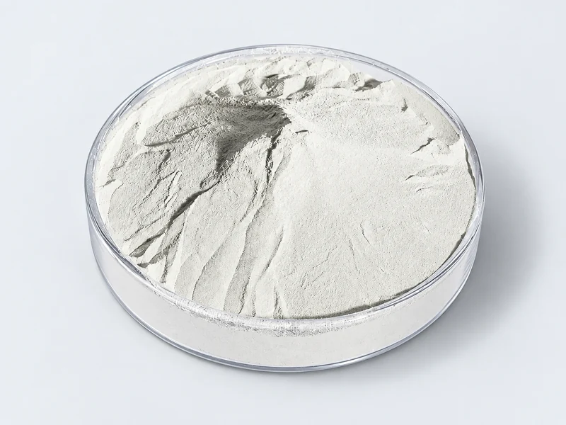
Composition defines the dielectric material system selected for the design.
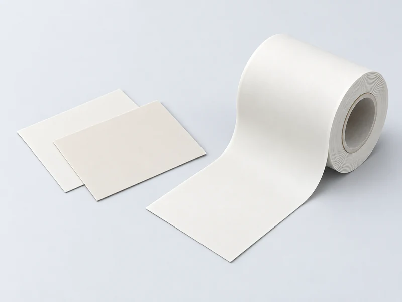
Unfired tape provides the layers for circuit printing, stacking and lamination.
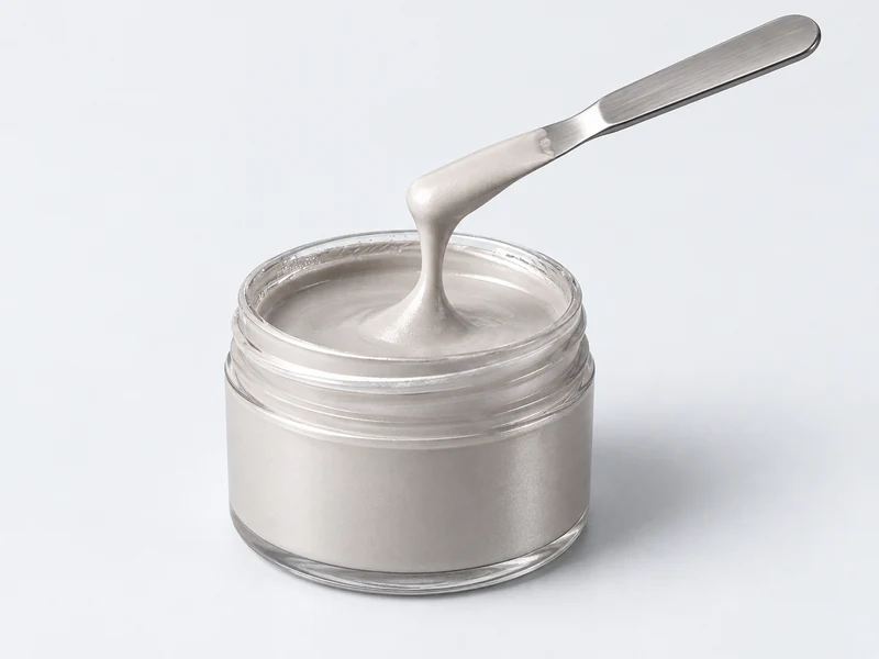
Matching paste forms printed conductors within the co-fired material system.
Materials are evaluated together through stacking and firing. Process principle, not a device specification.
Material synthesis, tape casting and heterogeneous co-firing are developed as one route, so evaluation can address both material properties and processing compatibility.
A published portfolio spanning low-dielectric, low-loss and high-strength options.
Compare the material dataClass 10,000 space supports automated tape casting and multilayer process development.
See the evaluation capabilitiesPowder characterization, green-tape development and matching-paste evaluation connect to multilayer process verification.
Discuss a material combinationA joint advanced functional ceramic materials and components R&D center supports specialist material and process development.
Published platform capacities are not a production allocation. Tape format, material system and project availability are confirmed during evaluation.
LTCC stands for Low Temperature Co-fired Ceramic. It is a material and manufacturing platform used to build compact multilayer electronic structures by printing conductors and circuit features on unfired ceramic tape, stacking the layers and firing them together.
The technology enables integration from material and circuit to package and system, supporting smaller, more integrated and modular electronic products.
Lead- and cadmium-free material options designed for co-firing with matching silver electrode paste. Final values are confirmed against the applicable product datasheet and test method.
Frequency is included with the dielectric-constant value. Loss, strength and firing values remain as published; request the relevant test method and specimen conditions before comparing systems or releasing a design.
All published grades are available below. Filter by series or grade name, then select up to four entries to compare. Final selection requires review of the complete operating conditions.
Scroll to view more columns.
| Grade | Positioning | Dielectric Constant | Loss | CTE ppm/°C | Flexural MPa | Firing °C |
|---|---|---|---|---|---|---|
| L3B9 | Ultra-low Dk, high-frequency low loss | 3.9 ±0.1 (10–40 GHz) | ≤0.002 | 2.3 | >100 | 875 |
| L4D4 | Low Dk, high-frequency low loss | 4.4 ±0.1 (8–40 GHz) | ≤0.002 | 4.1 | >125 | 850 |
| L4A9 | Low Dk, high-frequency low loss | 4.8 ±0.1 (@12 GHz) | ≤0.002 | 4.5 | >150 | 850 |
| L4C9 | Low dielectric constant | 4.85 ±0.1 (@12 GHz) | ≤0.0035 | 4.5 | >150 | 850 |
| L5A9 | Low Dk, high-frequency low loss | 5.9 ±0.1 (10–40 GHz) | ≤0.002 | 5.3 | >170 | 875 |
| L7HW | High strength | 7.0 ±0.1 (@10 GHz) | ≤0.0025 | 6.0 | >300 | 850 |
| L7H4 | High strength | 7.4 ±0.1 (@10 GHz) | ≤0.003 | 6.1 | >300 | 850 |
| L7BT | High CTE, high-frequency low loss | 7.7 ±0.2 (10–40 GHz) | ≤0.001 | 12.5 | >200 | 900 |
| L7H8 | High strength | 7.8 ±0.1 (@10 GHz) | ≤0.0025 | 6.3 | >300 | 875 |
| L15A0 | Mid-Dk, low loss | 15.0 ±0.5 (@10 GHz) | ≤0.001 | 9.6 | >150 | 900 |
| L25A0 | Mid-Dk, ultra-low loss | 26.0 ±0.5 (@10 GHz) | ≤0.00025 | 9.2 | >200 | 900 |
| L40C0 | Medium-high Dk, low loss | 38.5 ±1 (@10 GHz) | ≤0.0006 | 7.9 | >200 | 900 |
Dielectric properties are frequency-dependent. Custom dielectric ceramic material development is available for qualified projects.
Composition, particle size, structure and processing behavior are assessed with complementary methods.
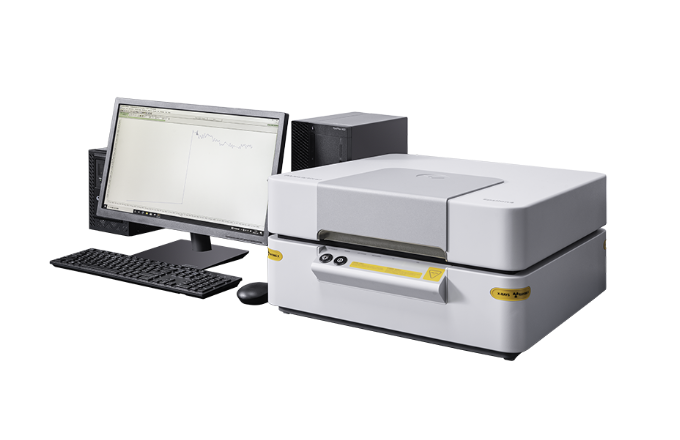
XRF analysis supports review of material composition.
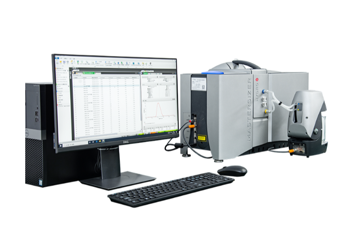
Laser analysis characterizes the powder particle-size distribution.
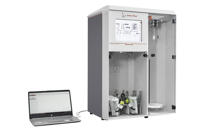
Surface-area measurement supports powder characterization.
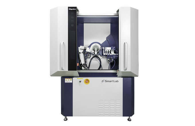
X-ray diffraction supports crystalline-phase analysis.
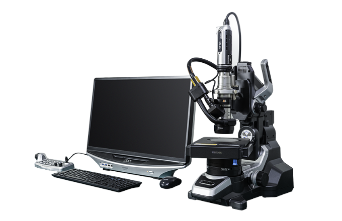
3D microscopy supports surface and dimensional review.
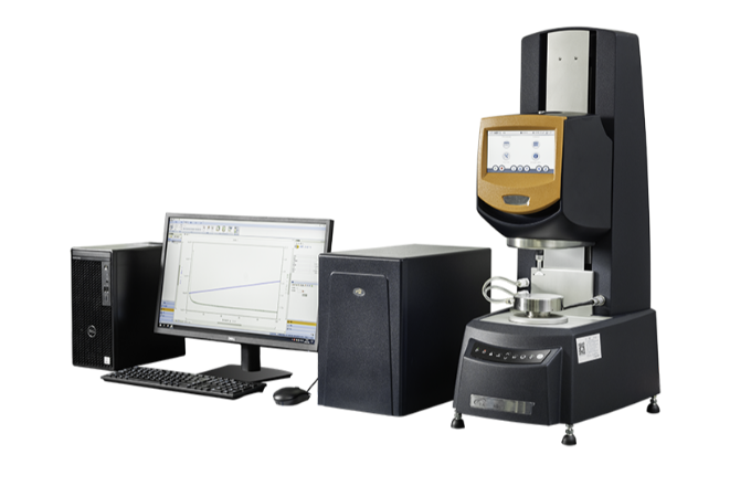
Rheology testing supports review of slurry processing behavior.
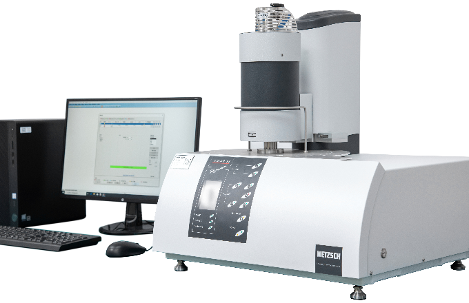
Thermomechanical analysis supports material characterization with temperature.
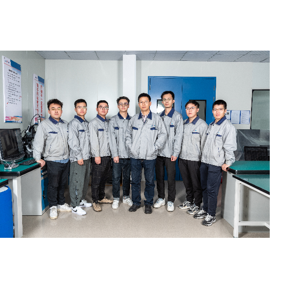
Specialist material and process work connects formulation with evaluation.
| Dielectric material | LTCC powder and green tape |
|---|---|
| Metallization | Matching silver electrode paste |
| Development | Custom dielectric formulations by project |
| Validation | Application and multilayer process verification |
| Compliance | RoHS-oriented, lead- and cadmium-free material options |
Send the dielectric target, operating frequency, tape format, electrode system and annual demand for technical review and factory-direct pricing.